
|
|
|
Current Research:The technological realization of many novel electronic devices such as single electron transistors, quantum dot lasers, and solid state quantum computers will ultimately rely on the growth of self assembled arrays of nanometre sized structures. Control of defects and growth of nanostructures on surfaces is also central to the future success of a wide range of other technological developments including new sensors, advanced thin film growth, and novel catalysts. In the Surface Nanoscience research group we study and control materials on the atomic and nanometre scale. This deepens our understanding of the role of defects and nanostructures in existing materials, as well as leading to the creation of new materials with novel chemical, electronic, magnetic, and optical properties. Oxide nanostructures One of the most promising current areas in nanoscience that is likely to become a widespread technology is to simultaneously create billions of active nanometre scale features through chemical self assembly. Electronic processors and memory built through a combination of self assembly and lithography will have a much higher component density and be orders of magnitude faster and cheaper than those created with current techniques. Should it become possible to exercise sufficient control over the nanostructures and interactions of electrons confined in them it will also be possible to use them as the fundamental building blocks for devices whose operation is based on quantum interactions. 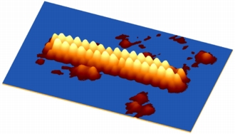
Our work on SrTiO3 has shown that local non-stoichiometry in the surface region of these crystals gives rise to non-perovskite phases which appear as either nanolines or nanodots. Both these nanostructure types are highly regular and self assemble into arrays. The figure on the right is a 3D rendered STM image of an isolated nanoline that is 12 nm long and around 1 nm wide. The bright orange peaks are individual atoms. Our Auger electron spectroscopy analysis shows that these nanostructures are composed of TiO2 units (image by Martin Castell). Our current activities are directed at the study of the electrical and optical properties of the nanostructures to determine whether quantum confinement is taking place. We have used them as templates for the growth of metallic nanocrystals and for the ordering of fullerenes. Possible applications in gas sensor devices and for heterogenous photocatalysis are also being considered. Metal nanocrystals
The aim now is to take this work forward for a variety of metals and correlate the properties of interest with the nanocrystal shape. For example, optical resonances of Au nanocrystals depend on the cluster size, but the influence of shape has not been studied to date. Tighter and stronger resonances may be possible if shape control is added to size and distribution control. The catalytic activity of nanoparticles is also known to depend on particle size, and we are interested in correlating the particle shape with activity. If certain shapes are shown to be more catalytically active this paves the way for more efficient catalysts. Another application would be to use nano-structured surfaces created on insulating oxides to be used as a template for the growth of metallic islands. If the island growth is constrained by the template then it might be possible to create a well ordered array of nanometre sized metal islands that could otherwise not be achieved. Molecular ordering
Further work in this area will expand on the molecules and templates. For example, if conducting molecules ordered themselves preferentially in a similar way to the fullerenes then one would have achieved a way of creating nanowires of a single molecular width. This type of work would be of great interest to researchers active in molecular and nano-electronics. Other applications are the ordering of functional molecules to be used as bits in devices with possible applications in quantum information processing technologies. Together with Professor Don Fraser from Earth Sciences we are also investigating the ordering of organic bases such as adenine on perovskite surfaces. We hope to see if these molecules can be encouraged to form linear chains. Surface structure of dielectric materials and thin films
Over the last 9 years we have studied the surface structure of SrTiO3 on the atomic scale, in particular the (001), (011), and (111) surface reconstructions. On the right is an STM image of the SrTiO3 (111) surface showing the (6x6) and (4x4) reconstructions (image by Martin Castell). We now intend to take this work further by studying SrTiO3 film growth with in-situ STM. The intention is then to expand that activity to other dielectric materials and to establish the relationship between dielectric thin film growth/processing conditions and the atomic scale structure of the films with a view to tailoring their performance according to the application. Dopant mapping in semiconductors
Dopant imaging with secondary electrons is likely to become an important technique in the semiconductor industry. To build on our activity in this field we intend to further develop dopant imaging and obtain quantitative information from Si and III-V heterostructures and devices. In principle it is possible to image individual defect and dopant sites with the secondary electron signal, but to achieve this, precise control over surface conditions is necessary so that imaging needs to be carried out in an ultra high vacuum environment. With decreasing device sizes the statistical dopant distribution becomes significant, so it is technologically important to study dopant incorporation at growth temperatures. Through the combined use of scanning tunnelling microscopy and secondary electron imaging we intend to observe in-situ dopant incorporation, defect generation, and defect evolution during epitaxial growth of semiconductors. |
 Supported metal crystals of nanometre dimensions have a bewildering breadth of applications.
Noble metals are in widespread use as catalysts, Ag and Au can be used for optical applications,
and magnetic metals have possible
applications in ultra high density information storage media.
A central issue is the control of the size and distribution of the nanocrystals. A more demanding
goal is to be able to select the nanocrystal shape, but we have recently shown how the shape of
nanocrystalline Pd can be accurately controlled. We
have also discovered that Au can grow in a bimodal manner on an oxide surface. The scanning
tunnelling microscope image on the
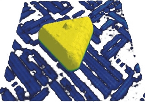
right shows a Pd nanocrystal with 8 nm edge length
on a nanostructured SrTiO3 support. We find
that these crystals can be encapsulated with a thin TiOx overlayer
(image by Fabien Silly).
Supported metal crystals of nanometre dimensions have a bewildering breadth of applications.
Noble metals are in widespread use as catalysts, Ag and Au can be used for optical applications,
and magnetic metals have possible
applications in ultra high density information storage media.
A central issue is the control of the size and distribution of the nanocrystals. A more demanding
goal is to be able to select the nanocrystal shape, but we have recently shown how the shape of
nanocrystalline Pd can be accurately controlled. We
have also discovered that Au can grow in a bimodal manner on an oxide surface. The scanning
tunnelling microscope image on the
right shows a Pd nanocrystal with 8 nm edge length
on a nanostructured SrTiO3 support. We find
that these crystals can be encapsulated with a thin TiOx overlayer
(image by Fabien Silly).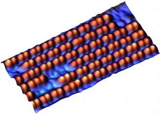 The packing arrangement of molecules on surfaces depends on a variety of factors including
molecular shape, molecule - molecule interactions, and molecule - substrate bonding.
We are currently working on schemes to use nanostructured oxide surfaces as templates to influence
molecular packing. An example of this is the self assembly of fullerenes into chains
and square packing configurations, which are unusual packing arrangements. Fullerenes normally form
close packed islands on surfaces. The STM image on the right (taken by David Deak) shows endohedral
fullerenes (Er3N@C80) that have been ordered into
a rectangular array through co-ordination with an (8x6) 'waffle' template on the
SrTiO3 (001) surface. The molecules have been coloured orange and
are around 1 nm in size.
The packing arrangement of molecules on surfaces depends on a variety of factors including
molecular shape, molecule - molecule interactions, and molecule - substrate bonding.
We are currently working on schemes to use nanostructured oxide surfaces as templates to influence
molecular packing. An example of this is the self assembly of fullerenes into chains
and square packing configurations, which are unusual packing arrangements. Fullerenes normally form
close packed islands on surfaces. The STM image on the right (taken by David Deak) shows endohedral
fullerenes (Er3N@C80) that have been ordered into
a rectangular array through co-ordination with an (8x6) 'waffle' template on the
SrTiO3 (001) surface. The molecules have been coloured orange and
are around 1 nm in size..jpg) Dielectric materials such as SrTiO3 are used in
dynamic random access memory applications and have been proposed as a gate
dielectric to replace SiO2 in complementary metal oxide semiconductor devices.
The reason for incorporating complex oxides into high performance microelectronics
is that they have significantly higher relative permittivities than in the materials
that are currently used. With the ever shrinking nature of microelectronics the
pressure on controlling the processing steps has reached the point where the
semiconductor industry is looking at controlling materials on a near atomic scale.
Just a few atoms out of place can make the difference between a device that operates
as it should and one that fails.
Dielectric materials such as SrTiO3 are used in
dynamic random access memory applications and have been proposed as a gate
dielectric to replace SiO2 in complementary metal oxide semiconductor devices.
The reason for incorporating complex oxides into high performance microelectronics
is that they have significantly higher relative permittivities than in the materials
that are currently used. With the ever shrinking nature of microelectronics the
pressure on controlling the processing steps has reached the point where the
semiconductor industry is looking at controlling materials on a near atomic scale.
Just a few atoms out of place can make the difference between a device that operates
as it should and one that fails.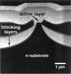 The key atoms that control electrical activity in semiconductors are called dopants.
These are deliberately introduced impurity atoms that supply electrons or holes, which
move freely through the crystal. One of the current major challenges in the semiconductor
industry is to develop new techniques that will map dopant distributions at high spatial
resolution and with high sensitivity. Together with Professor Doug Perovic at the
University of Toronto we have pioneered a technique for imaging dopants
using the secondary electron signal in the scanning electron microscope. An example of
this technique is shown in the secondary electron image of a cross section through
an InGaAsP laser. The image shows two p-type channels rising up through the n-type substrate
(image by Cordelia Sealy).
The key atoms that control electrical activity in semiconductors are called dopants.
These are deliberately introduced impurity atoms that supply electrons or holes, which
move freely through the crystal. One of the current major challenges in the semiconductor
industry is to develop new techniques that will map dopant distributions at high spatial
resolution and with high sensitivity. Together with Professor Doug Perovic at the
University of Toronto we have pioneered a technique for imaging dopants
using the secondary electron signal in the scanning electron microscope. An example of
this technique is shown in the secondary electron image of a cross section through
an InGaAsP laser. The image shows two p-type channels rising up through the n-type substrate
(image by Cordelia Sealy).